

HT12D Decoder IC for Remote Control Systems
Contents
HT12D is a 212 series decoder IC (Integrated Circuit) for remote control applications manufactured by Holtek. It is commonly used for radio frequency (RF) wireless applications. By using the paired HT12E encoder and HT12D decoder we can transmit 12 bits of parallel data serially. HT12D simply converts serial data to its input (may be received through RF receiver) to 12 bit parallel data. These 12 bit parallel data is divided in to 8 address bits and 4 data bits. Using 8 address bits we can provide 8 bit security code for 4 bit data and can be used to address multiple receivers by using the same transmitter.
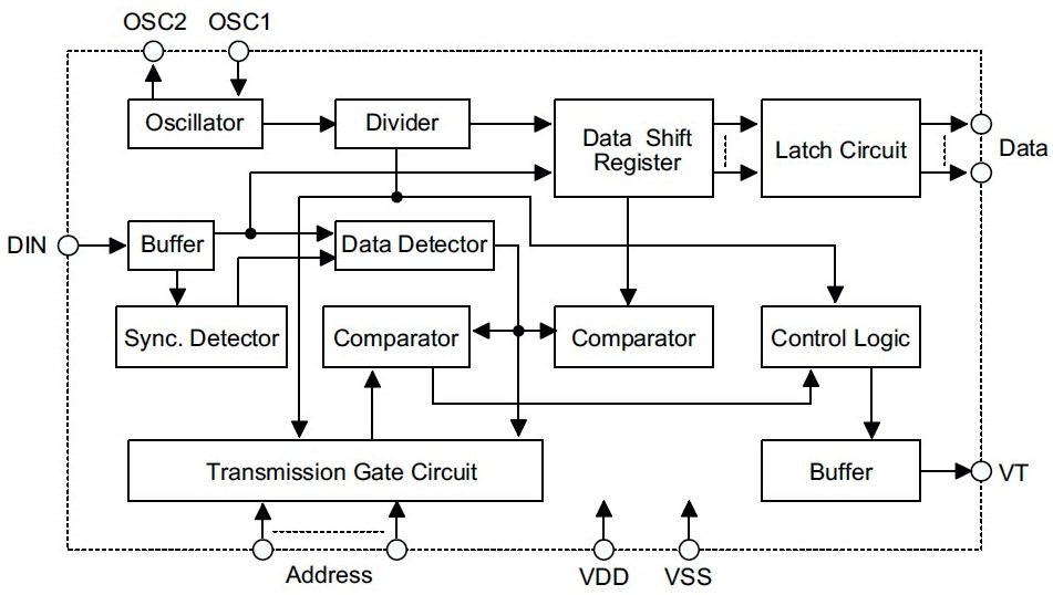
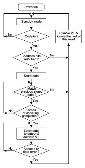
HT12D is a CMOS LSI IC and is capable of operating in a wide voltage range from 2.4V to 12V. Its power consumption is low and has high immunity against noise. The received data is checked 3 times for more accuracy. It has built in oscillator, we need to connect only a small external resistor. As HT12E, it is available in 18 pin DIP (Dual Inline Package) and 20 pin SOP (Small Outline Package) as given below.
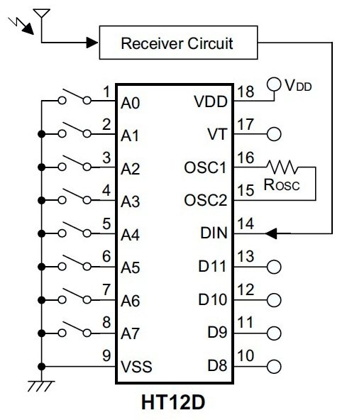
Pin Diagram and Description
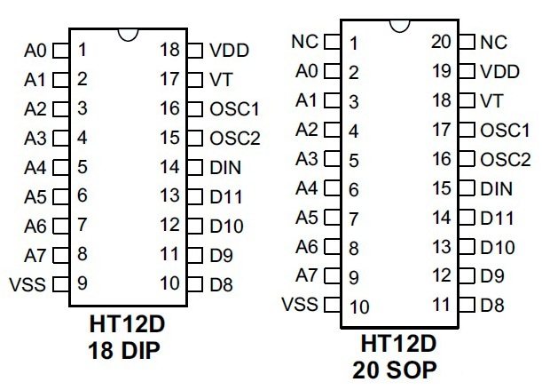
- VDD and VSS are used to provide power to the IC, Positive and Negative of the power supply respectively. As I said earlier its operating voltage can be in the range 2.4V to 12V
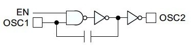
- OSC1 and OSC2 are used to connect external resistor for internal oscillator of HT12D. OSC1 is the oscillator input pin and OSC2 is the oscillator output pin as shown in the figure below.
- A0 – A7 are the address input pins. Status of these pins should match with status of address pin in HT12E (used in transmitter) to receive the data. These pins can be connected to VSS or left open.
- DIN is the serial data input pin and can be connected to a RF receiver output.
- D8 – D11 are the data output pins. Status of these pins can be VSS or VDD depending upon the received serial data through pin DIN.
- VT stand for Valid Transmission. This output pin will be HIGH when valid data is available at D8 – D11 data output pins.
Working
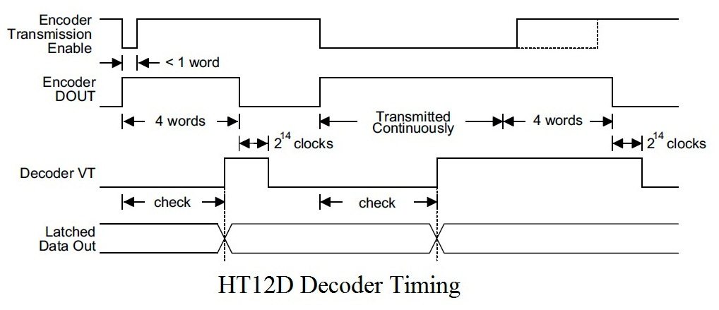
HT12D decoder will be in standby mode initially ie, oscillator is disabled and a HIGH on DIN pin activates the oscillator. Thus the oscillator will be active when the decoder receives data transmitted by an encoder. The device starts decoding the input address and data. The decoder matches the received address three times continuously with the local address given to pin A0 – A7. If all matches, data bits are decoded and output pins D8 – D11 are activated. This valid data is indicated by making the pin VT (Valid Transmission) HIGH. This will continue till the address code becomes incorrect or no signal is received.
Typical Application Circuit
Use Rosc 51KΩ as recommended in the datasheet.


Can we simulate this in any of the simulating software with the transmission and receiver module connected? If yes, then in which software?
Yes.. it is matched..
Similarly you may connect A0 ~ A7 of both ICs to VCC
Sorry to bother, the A0-A7 of both ICs are grounded. Is it matched now?
You can set the address in HT12D and HT12E ICs, just by providing HIGH and LOW to its inputs.
Really helpful, I’ll share this with my buddies.
And ‘the A0- A7 address should match with encoder address.’ How to do this matching??